")

-
silicon carbide (SiC) technology – thermal oxidation, reactive ion etching, metal/semiconductor contacts;
-
manufacturing using PECVD, ALD and magnetron sputtering techniques, thermal treatment and characterization of dielectric layers with high electrical permittivity;
-
characterization of broadband semiconductor materials - defect structure, surface condition, junctions, characterization of electrically active defects in cryogenic temperatures using DLTS and TSC techniques;
-
design, modeling, manufacturing and characterization of high-power and high-frequency devices in broadband semiconductor technologies (SiC, GaN, diamonds) - Schottky diodes, PiN diodes, MOSFET transistors;
-
construction of power electronic converters using power devices in SiC and GaN (gallium nitride) technologies;
-
production and characterization of heterostructures and heterojunction devices for photodetection of UV, visible, gamma radiation and particles (ZnO, SiC, GaN, AlN, others);
-
fiber optic sensors: refractive index, pressure, temperature, biosensors;
-
production of layers for sensing applications employing vapor deposition techniques;
-
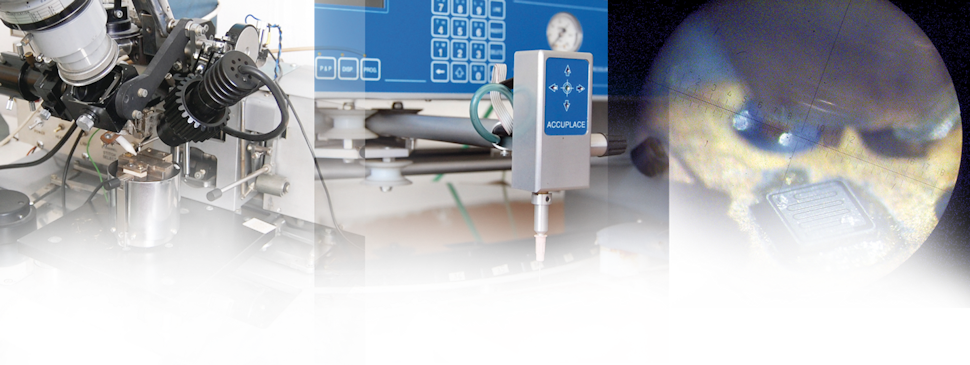
SMD assembly technology on rigid, semi-rigid and flexible laminates, laser cut templates for paste screen printing, rigid and flexible laminates, semiconductor and glass substrates, reliability tests of printed circuits;
-
technology for semiconductor devices microassembly.
 |
Head of Electronic Materials And Microsystem Technology Division Mariusz Sochacki, PhD, DSc tel: (+48) 22 234 7932 e-mail: Electrical Engineering Building (GR), room no. 423C |
Electronic Materials And Microsystem Technology Division website: http://zmime.imio.pw.edu.pl