#P-32
GST phase change material for photonic applications
Alicja KĄDZIELA, Dagmara DRECKA, Michał GOLAS, Marcin JUCHNIEWICZ, Marcin LELIT,
Bartłomiej STONIO, Mateusz SŁOWIKOWSKI, Piotr WIŚNIEWSKI
Politechnika Warszawska, Centrum Zaawansowanych Materiałów i Technologii CEZAMAT,
ul. Poleczki 19, 02-822 Warszawa
Phase-change materials (PCMs), particularly those based on chalcogenide compounds like Ge2Sb2Te5 (GST), offer significant potential for tunable optical components in nanophotonic circuits. These materials can be rapidly and reversibly switched between amorphous and crystalline phases using low-energy optical or electrical pulses, resulting in a substantial refractive index contrast (∆n > 1) across a broad wavelength range, from visible to infrared (IR). This unique property makes PCMs highly promising for on-chip photonic memories and versatile applications, especially in telecom and mid-IR wavelengths where low loss is critical. In this work, we present the experimental results of optimizing the GST layer and numerical simulations of the SiN waveguides with an integrated GST layer on top.
GST thin films were deposited on silicon substrates by magnetron sputtering. Amorphous samples were annealed in rapid thermal processing (RTP) system at different temperatures. In order to investigate optical properties of specimens, ellipsometric measurements were performed. In Fig. 1 n (a) and k (b) characteristics of samples annealed in different temperatures are plotted and manifest great changes during the phase changing process. The curves can be distinguished in three areas, corresponding to three different GST phases (amorphous, fcc, hcp). A tendency was observed for the optical constants values to increase with increasing annealing temperature. Simulations of field distribution and propagated modes were conducted in the Lumerical FDE solver for a 400 nm x 1 µm SiN waveguide. The waveguide, surrounded by a GST layer and encompassed by SiO2, was modeled in 2D for 1550 nm using obtained ellipsometry data. Electric field distribution of the fundamental TE mode (mode 0) for a SiN waveguide with a 32,5 nm layer of amorphous GST and crystallized GST at 170°C is presented in Figure 1. Images show visible differences in guided mode, affecting transmission through such a structure depending on GST layer state.
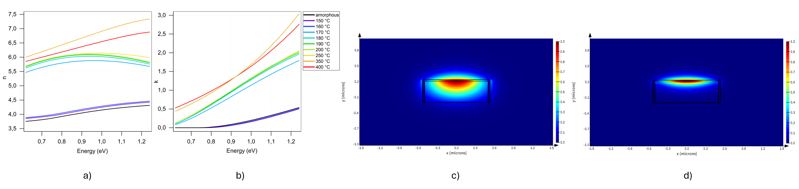
Fig. 1. Optical constants of GST samples: a) refractive index, b) extinction coefficient;
Electric field distribution of the fundamental TE mode for a waveguide with: c) amorphous and d) crystallized GST.
References
[1] P. Prabhathan, et al. "Roadmap for phase change materials in photonics and beyond." Iscience 26.10 (2023).