Van der Waals heterostructures for next generation nano and optoelectronics
Małgorzata Giza
supervisor: Mariusz Zdrojek
Due to electrical, optical, and thermal properties, two-dimensional materials are widely studied in the field of modern electronics and optoelectronics. However, despite the promising results, atomically thin layers have some limitations (sensitivity to the environment, formation of the Schottky barrier in the metal-semiconductor junction) that can affect the performance of the devices. Such negative features can be overcome by stacking layers of different 2D materials into a van der Waals heterostructure (Fig. 1 top left, bottom). Therefore, we can obtain a completely new material that will have the properties of the component layers.
This research is focused on the fabrication of van der Waals heterostructures and the study of their structural and electrical properties. For this purpose, the method of gold-assisted mechanical exfoliation was used, which allows the production of large-area continuous layers of TMDs (Fig. 1 top right). The layers are stacked on top of each other using a 2D material transfer system. Next, it is possible to produce devices such as transistors or photodetectors on the obtained heterostructures using e-beam lithography. The large area of the material is a great advantage, because it enables the production of multiple devices on a heterostructure made of the same layers, allowing a reliable comparison of their performance.
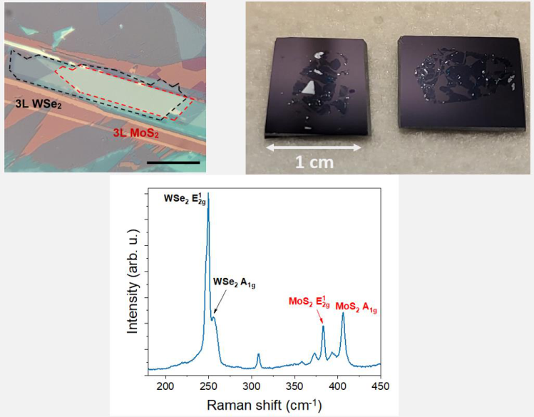
Fig. 1 (Top left) Example of fabricated MoS2/WSe2 heterostructure (L – layer, scale bar 50 μm). (Top right) Mechanically exfoliated large-area flakes of MoS2 monolayer. (Bottom) Raman spectrum of MoS2/WSe2 heterostructure.