Simulations and design of germanium-based photonic integrated elements working in mid-infrared spectral range
Marcin Lelit
supervisor: Ryszard Piramidowicz
The interest in mid-infrared photonics is focused on sensing applications due to presence of strong absorption lines of gasses and liquids [1] i.e. CO2, NOx, SOx. One of material platform used for such applications is germanium-on-silicon (Ge-on-Si) which provide refractive index contrast of 0.7 at at 3.8 µm [2]. This work reports early stages of development of Ge-on-Si photonic integrated photonic platform operating in range from 3.0 to 5.2 µm. Two sets of test elements and topographies were designed, one series of test structures was manufactured and is under characterization process.
First stage in development of photonic integrated platform, after the material is chosen, are numerical simulations of straight waveguides and bends to determine basic geometrical constraints of the elements. Two different heights of germanium were considered: 1 and 2 µm. Examples of mode profiles with fully etched waveguides cross-sections are presented in Figure 1.
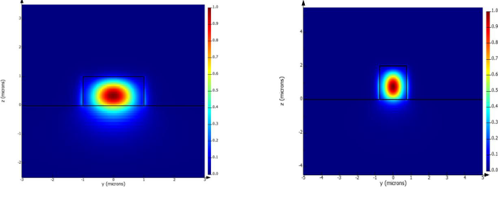
Fig. 1 (a) mode profile for waveguide H = 1 μm, W = 2 μm at λ = 5.2 μm ; (b) mode profile for waveguide H = 2 μm, W = 1.5 μm at λ = 5.2 μm.
In the second stage of design process, grating couplers geometries were optimized for full etch process and for shallow etch in 2 µm germanium layer. Theoretical efficiencies up to 20% were achieved with potential for further improvement with more complex material stack that emulates substrate refractive index equal 2.
[1] A. Malik, M. Muneeb, Y. Shimura, V. J. Campenhout, V. D. R. Loo, i G. C. Roelkens, „Germanium-on-silicon planar concave grating wavelength (de) multiplexers in the mid-infrared”, Applied Physics Letters, t. 103, nr 16, s. 161119–1/4, 2013, doi: 10.1063/1.4826114.
[2] W. Li i in., „Germanium-on-silicon nitride waveguides for mid-infrared integrated photonics”, Appl. Phys. Lett., t. 109, nr 24, s. 241101, grudz. 2016, doi: 10.1063/1.4972183.