Influence of 2-dimensional interlayer on contact resistance in TMD-based field-effect transistors
Małgorzata Giza
supervisor: Mariusz Zdrojek
The electrical contacts to two-dimensional semiconductors such as Transition Metal Dichalcogenides are still a main limiting factor in the device’s performance. This significant bottleneck in an efficient current injection into the 2D active layers is due to the formation of the Schottky barrier. In order to reduce the Schottky barrier height, one can put an additional layer (interlayer) between the metal and 2D semiconductor.
This research is focused on studying the influence of interlayers on contact resistance in TMD-based field-effect transistors. For this purpose, using the gold-assisted mechanical exfoliation method, large-area TMDs monolayers are produced and shaped with e-beam lithography. The large area of the material enables the fabrication of multiple devices on the same layers, allowing for a reliable comparison of their performance. Using 2D materials transfer system, the additional layer is placed only on the contact area of the device. Then the metal layer is thermally evaporated on top of the contact structure. In this way, one can obtain monolayer back-gate transistors with a 2D interlayer under metal contact (Fig.1). Devices are designed in TLM architecture with channel lengths under 4,5 µm, which allows for accurately determining contact resistance. The results of this work contribute to improvement in contact engineering strategy which leads to enhanced performance of 2D TMDs-based devices.
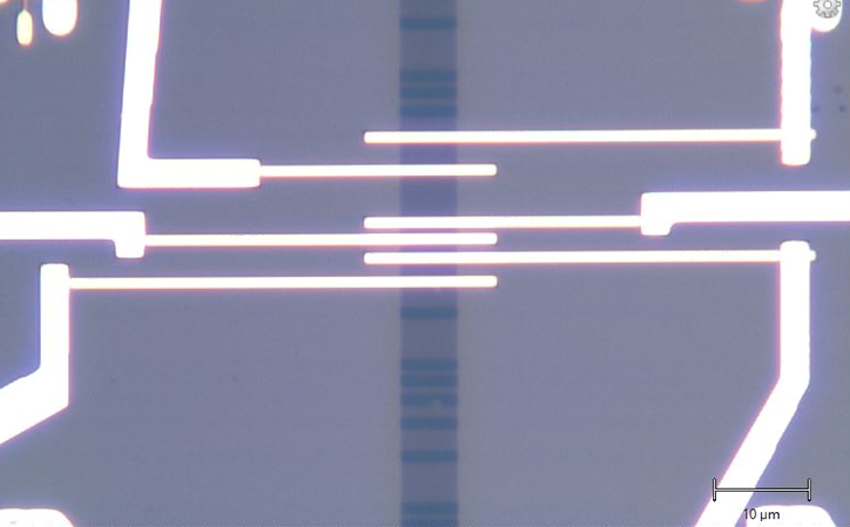
Fig. 1 1L-WS2 field-effect transistors with 1L-MoS2 interlayer under contact.