Advances in development of germanium-based mid-infrared passive photonic platform
Marcin Lelit
supervisor: Ryszard Piramidowicz
The interest in mid-infrared photonics is focused on sensing applications due to presence of strong absorption lines of gasses and liquids [1] i.e. CO2, NOx, SOx. One of material platform used for such applications is germanium-on-silicon (Ge-on-Si) which provide refractive index contrast of 0.7 at 3.8 µm [2]. This work reports advances in development of Ge-on-Si photonic integrated photonic platform operating in range from 3.0 to 5.2 µm. Waveguides, tapers, grating couplers (GCs) and Arrayed Waveguide Gratings (AWGs) de-/multiplexes were designed. First series of photonic integrated circuits (PICs) comprising test structures was manufactured and is under characterization process.
GCs allow for vertical coupling and decoupling of light without need for PICs dicing. AWGs which are the most complex type of passive photonic elements. Colourless AWGs with 8 output channels and wide channel spacing of 40 to 50 nm are designed in the first set.
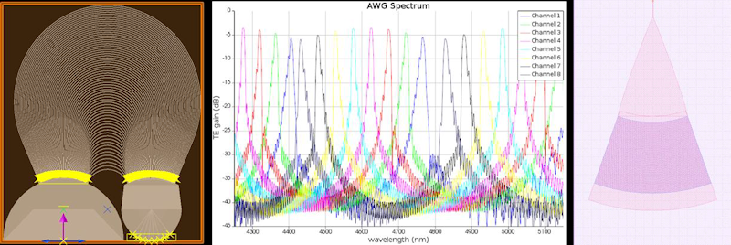
Fig. 1 AWG layout (a); AWG spectrum (b); Grating Coupler layout (c).
In the second stage of design process, GCs and AWGs geometries are optimized for shallow etch in 2 µm germanium layer. Theoretical efficiencies of GCs up to 20% were achieved with potential for further improvement with more complex material stack.
This work received support from the National Centre for Research and Development through MIRPIC project (TECHMATSTRATEG-III/0026/2019-00).
References
[1] A. Malik, M. Muneeb, Y. Shimura, V. J. Campenhout, V. D. R. Loo, and G. C. Roelkens, “Germanium-on-silicon planar concave grating wavelength (de) multiplexers in the mid-infrared,” Applied Physics Letters, vol. 103, no. 16, pp. 161119–1/4, 2013, doi: 10.1063/1.4826114.
[2] W. Li et al., “Germanium-on-silicon nitride waveguides for mid-infrared integrated photonics,” Appl. Phys. Lett., vol. 109, no. 24, p. 241101, Dec. 2016, doi: 10.1063/1.4972183.