Diffusion of electrically active and total Si in GaAs investigated separately using depth-profiling techniques
Adrianna Wójcik
supervisor: Włodzimierz Strupiński
Progressing miniaturization of electrical devices dimensions requires constant development of characterization techniques. Standard dynamic Secondary Ion Mass Spectrometry (SIMS) provides depth profiles of impurity atoms without distinguishing electrically active and inactive parts. Whereas Electrochemical Capacitance Voltage (ECV) technique yields depth profiles of all carriers present in the structure. The observation of significant discrepancies between the profiles measured by these two techniques, which exceeds their measurement uncertainty, sparks the discussion on the varying diffusion of electrically active and inactive impurities.
In this work GaAs:Si sample was investigated using a combination of depth-profiling techniques. The shape of a carrier profile obtained by ECV was found to be in good agreement with the As-Six profile measured by Ultra Low Impact Energy SIMS (ULIE-SIMS) depth profiling confirming that these two techniques can be used interchangeably. However, the superior depth resolution of ULIE-SIMS allows to access nanometers-thick structures.
SIMS and ULIE-SIMS results obtained for the sample annealed at 800°C for 30 minutes revealed that the electrically active and total impurity distributions in the sample significantly vary. The analysis based on Fick’s laws allowed for quantitative comparison of the diffusion rates of electrically active and total Si, and for preparing further work plans for an in-depth study of Si diffusion.
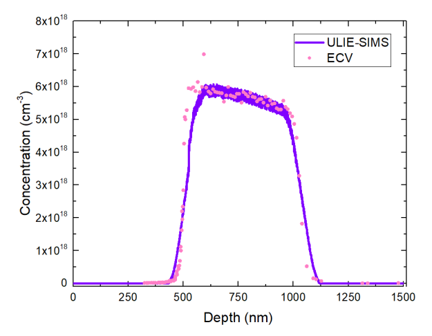
Fig. 1 VECV carrier profile and ULIE-SIMS active Si profile obtained for GaAs:Si sample.